Introduction
Printed Circuit Boards (PCBs) form the base of most electronic devices. They connect electronic parts and help them work together. You can find PCBs in computers, phones, cars, medical devices, and many other products.
Designing a PCB takes careful planning. Engineers must place parts, create electrical paths, and check every connection. They must also make sure the board fits its case and works as planned.
PCB design software helps engineers handle these tasks. It provides tools for drawing circuits, placing components, routing tracks, and checking designs. Some tools also support 3D views and manufacturing files.
However, every software package offers different features. Some work well for beginners and small projects. Others support large designs and complex electronic products.
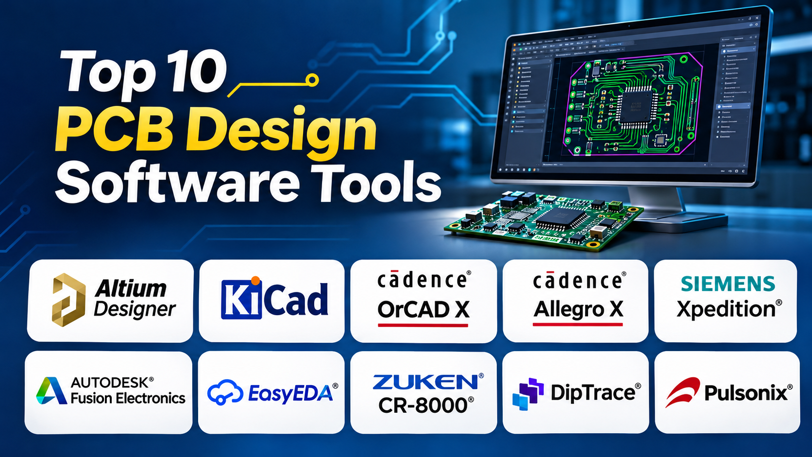
This guide explains ten popular PCB design software tools. It covers their main features, uses, advantages, and limitations. It also helps you compare them before making a choice.
What Is PCB Design Software?
PCB design software helps users create printed circuit board layouts. It turns an electronic circuit plan into a board that manufacturers can produce.
The process starts with a circuit diagram. This diagram shows how electronic parts connect. Users then move to the board layout and place each part in the right position.
Next, they connect the parts with copper tracks. These tracks carry electrical signals and power across the board.
Good PCB software also checks the design. It can find problems such as short circuits, missing connections, and spacing errors. These checks help reduce mistakes before production.
Many tools also create manufacturing files. These files tell factories how to make the board. Some programs offer 3D views, team tools, and component libraries.
Key Features to Look for in PCB Design Software
Before choosing a tool, understand the features that matter most.
1. Schematic Design
A schematic shows how electronic parts connect. It uses symbols for parts such as resistors, capacitors, chips, and connectors.
A good schematic editor helps users draw and manage these connections. It should also make it easy to find errors and update the circuit.
2. PCB Layout and Component Placement
PCB layout tools help users place parts on the board. Users must consider board size, part direction, heat, and signal paths.
Good placement can make routing easier. It can also improve board performance and reduce design problems.
3. Routing Tools
Routing connects components through copper tracks. Some tools offer automatic routing. Others provide manual routing tools for better control.
A good routing system should support different track widths, layers, and connection rules.
4. Design Rule Checks
Design Rule Checks (DRC) help find layout problems. They check track spacing, hole sizes, board edges, and other design limits.
These checks help users find errors before they send the design to a factory.
5. Component Libraries
Component libraries contain ready-made parts and their design details. They may include symbols, footprints, and 3D models.
A strong library saves time. It also helps users avoid mistakes when they select parts.
6. 3D Board Views
A 3D view shows how the finished board may look. Users can check component height, position, and fit.
This feature helps when a PCB must fit inside a product case.
7. Manufacturing Support
PCB software should create files that manufacturers can use. These may include Gerber files, drill files, and assembly data.
Clear manufacturing output helps reduce delays and production errors.
Top 10 PCB Design Software Tools
1. Altium Designer
Altium Designer is a professional PCB design platform. It brings circuit design, board layout, routing, and design checks into one workspace.
The software supports complex electronic projects. Engineers can use it to design multi-layer boards and manage large component libraries.
One of its main strengths is its connected design workflow. Users can move between the schematic and PCB layout. This helps them keep circuit connections and board changes in sync.
Altium Designer also offers advanced routing tools. These tools help engineers manage track paths, board layers, and design rules. They can also review the board in 3D.
The platform supports design checks throughout the process. These checks help users find electrical and layout problems early. This can reduce costly changes during production.
Key Features
- Schematic capture for drawing electronic circuits.
- PCB layout tools for placing and connecting components.
- Advanced routing for complex board designs.
- Multi-layer PCB support.
- Design Rule Checks for finding layout errors.
- 3D board views for checking component placement.
- Component libraries for managing electronic parts.
- Manufacturing output for board production.
- Design collaboration features for engineering teams.
Why Choose Altium Designer?
Altium Designer suits engineers who need a complete PCB design environment. It offers many tools for professional development work.
Its connected design process helps users manage changes. This can make large projects easier to control.
The software also supports detailed board checks. Engineers can review their work before sending it for production.
Pros
- Offers a wide range of professional design tools.
- Supports complex and multi-layer PCB projects.
- Connects schematic and PCB layout work.
- Provides advanced routing features.
- Includes useful 3D design views.
- Supports detailed design checks.
- Helps teams manage complex projects.
Cons
- Can cost more than many other PCB tools.
- New users may need time to learn it.
- Advanced features may feel complex at first.
- Large projects may need powerful computer hardware.
Best Suited For
Altium Designer works well for professional PCB engineers, electronics companies, and teams that design complex circuit boards.
2. KiCad
KiCad is a free and open-source electronic design platform. It offers tools for circuit diagrams, PCB layouts, and manufacturing preparation.
The software supports both simple and advanced projects. Students, hobbyists, engineers, and small businesses can use it.
KiCad includes a schematic editor. Users can draw circuits and connect electronic components. They can then move the design into the PCB editor.
Its PCB editor supports multiple copper layers. Users can place components, draw tracks, add board shapes, and set design rules.
KiCad also includes 3D viewing tools. These tools show the board with its components. Users can check the general shape and placement before production.
Another useful feature is its open-source nature. Users can work with the software without paying for a standard license. They can also access its source code and community resources.
Key Features
- Free and open-source software.
- Schematic editor for circuit design.
- PCB layout editor for board creation.
- Multi-layer PCB support.
- Electrical and design rule checks.
- 3D viewer for board inspection.
- Footprint and symbol libraries.
- Gerber and drill file generation.
- Custom design support.
Why Choose KiCad?
KiCad is a strong choice for users who want capable PCB tools without a software license cost.
It supports a complete design process. Users can create circuits, build board layouts, check designs, and prepare production files.
Its open-source model also gives users more freedom. Engineers can study, change, and share parts of the software.
Pros
- Free to use.
- Supports many types of PCB projects.
- Offers schematic and PCB design tools.
- Supports multi-layer boards.
- Includes 3D board viewing.
- Has an active user community.
- Does not require a paid license for standard use.
Cons
- Beginners may need time to learn the workflow.
- Some advanced tasks may need extra setup.
- Library management can take effort.
- Team workflows may need careful planning.
Best Suited For
KiCad suits students, hobbyists, independent engineers, startups, and small design teams that need flexible PCB software.
3. Cadence OrCAD X
Cadence OrCAD X is an electronic design platform for professional circuit and PCB development. It supports schematic capture, simulation, board layout, and design checks.
The platform helps engineers manage circuit designs before they move into production. Users can create circuit diagrams and check how parts connect.
Its simulation tools help users study circuit behavior. This can reveal problems before they build a physical board.
OrCAD X also supports PCB layout work. Engineers can place components and route electrical connections. They can use design rules to check spacing and other layout limits.
The platform works well for engineers who need more control over their design process. It also supports workflows that connect schematic design with PCB development.
Key Features
- Schematic capture for electronic circuit design.
- Circuit simulation tools.
- PCB layout and component placement.
- Routing tools for copper connections.
- Design Rule Checks.
- Component and library management.
- Manufacturing file preparation.
- Support for professional engineering workflows.
Why Choose Cadence OrCAD X?
OrCAD X suits engineers who need strong circuit design and analysis tools. Its simulation features help users study circuits before board production.
The platform also supports detailed PCB layout work. This makes it useful for products that need careful electrical design.
Engineers can use its design checks to find problems earlier. This can help save time during development.
Pros
- Provides strong schematic design tools.
- Supports circuit simulation.
- Includes PCB layout features.
- Offers design rule checking.
- Supports professional engineering work.
- Helps users study circuit behavior before production.
Cons
- New users may find the interface complex.
- Advanced functions can require training.
- Licensing costs may be high for some users.
- Users may need time to set up libraries and workflows.
Best Suited For
OrCAD X works well for electronics engineers, product development teams, and companies that need circuit analysis and PCB design tools.
4. Cadence Allegro X
Cadence Allegro X focuses on advanced PCB design. It supports complex boards that need careful routing, layer planning, and electrical control.
Engineers often use this type of software for demanding electronic products. These projects may include high-speed signals, dense component placement, and many board layers.
Allegro X offers tools for routing and managing complex connections. Engineers can control track paths and work with detailed design rules.
It also supports power and signal planning. This helps users manage how electrical power and signals move across the board.
The platform can handle designs with many components and connections. It also supports design checks that help users find layout problems.
Key Features
- Advanced PCB layout tools.
- High-density component placement.
- Multi-layer board design.
- High-speed routing support.
- Power and signal planning.
- Design Rule Checks.
- Advanced design constraint controls.
- Manufacturing output tools.
- Support for complex engineering projects.
Why Choose Cadence Allegro X?
Allegro X is useful when a board needs advanced layout control. It gives engineers tools for complex routing and detailed design constraints.
It can support products with many signals and components. This makes it suitable for demanding engineering work.
However, users should consider their project needs. Smaller projects may not need such a broad set of features.
Pros
- Supports complex PCB layouts.
- Offers advanced routing tools.
- Handles multi-layer designs.
- Provides detailed design constraints.
- Supports demanding electronic products.
- Helps engineers manage dense board layouts.
Cons
- Requires training and design experience.
- Can be costly for smaller teams.
- The large feature set may feel complex.
- May offer more tools than simple projects need.
Best Suited For
Allegro X suits experienced PCB engineers and companies that develop complex, high-speed, and high-density circuit boards.
5. Siemens Xpedition
Siemens Xpedition is a professional PCB design platform. It supports electronic system design, circuit development, and board layout.
The software helps teams manage complex electronic products. It brings design tasks into a connected engineering workflow.
Xpedition supports schematic capture and PCB layout. Engineers can place components and route connections across multiple board layers.
It also offers tools for design checks and collaboration. These features help teams review changes and manage design information.
Large projects often involve many engineers. Xpedition supports team-based work and helps users manage design tasks across a project.
Its design features can also help users manage electrical and mechanical needs. This matters when a board must fit inside a larger product.
Key Features
- Schematic design tools.
- PCB layout and routing.
- Multi-layer board support.
- Component placement tools.
- Design rule checking.
- Team collaboration features.
- Design data management.
- 3D design review.
- Support for complex electronic systems.
Why Choose Siemens Xpedition?
Xpedition suits companies that work on large electronic products. It provides tools for PCB design and team coordination.
Its design workflow helps engineers manage complex projects. Teams can review board details and work with shared design information.
The platform also supports detailed design checks. These checks help users find problems before manufacturing.
Pros
- Supports large PCB projects.
- Offers advanced design features.
- Helps teams manage shared work.
- Supports multi-layer boards.
- Provides design review tools.
- Works with complex electronic systems.
Cons
- Can be difficult for beginners.
- May require a large software budget.
- Setup and training can take time.
- Smaller teams may not need all its features.
Best Suited For
Siemens Xpedition suits large engineering teams, electronics manufacturers, and companies that develop complex products.
6. Autodesk Fusion Electronics
Autodesk Fusion Electronics combines electronic design with a wider product development environment. It helps users create circuit diagrams and PCB layouts.
The platform connects electronic design with mechanical product design. This is useful when a circuit board must fit inside a product case.
Users can create schematics and move them into PCB layouts. They can place components and route connections. They can also review the board in 3D.
This connected workflow helps designers check the relationship between the PCB and the product body. It can reveal space or fit problems before manufacturing.
Fusion Electronics also supports design libraries and manufacturing preparation. These features help users manage parts and prepare their boards for production.
Key Features
- Schematic capture.
- PCB layout and routing.
- Electronic and mechanical design connection.
- 3D PCB viewing.
- Component library tools.
- Design rule checks.
- Board design review.
- Manufacturing file preparation.
- Product development workflow support.
Why Choose Autodesk Fusion Electronics?
Fusion Electronics is useful for teams that design both electronic and mechanical products.
For example, a company may need to fit a PCB inside a small device. The software helps designers review the board and product case together.
This can reduce fit problems during product development. It also helps teams work across different design tasks.
Pros
- Connects electronic and mechanical design.
- Offers schematic and PCB layout tools.
- Supports 3D board review.
- Helps check product fit.
- Supports component libraries.
- Fits into a wider product design workflow.
Cons
- Users may need time to learn its full workflow.
- Some features depend on the chosen plan.
- Large projects may need careful setup.
- Users focused only on PCB design may prefer a dedicated tool.
Best Suited For
Fusion Electronics suits product designers, hardware startups, engineers, and teams that need electronic and mechanical design in one workflow.
7. EasyEDA
EasyEDA is a web-based electronic design platform. It helps users create circuit diagrams and PCB layouts through a browser.
Its simple access makes it useful for beginners and hobbyists. Users can start designing without setting up a large desktop application.
EasyEDA includes a schematic editor. Users can add electronic parts and connect them to create a circuit.
The PCB editor helps users arrange components and draw copper tracks. It also supports design checks and manufacturing file preparation.
The platform offers component libraries. These libraries help users find common parts for their designs.
EasyEDA also supports collaboration features. Users can share designs and work with other people. Its manufacturing workflow can help users move from design to board production.
Key Features
- Browser-based design environment.
- Schematic editor.
- PCB layout editor.
- Component libraries.
- PCB routing tools.
- Design rule checking.
- Multi-layer board support.
- Manufacturing file output.
- Design sharing and collaboration.
Why Choose EasyEDA?
EasyEDA is a useful option for users who want to start PCB design quickly. Its browser-based workflow makes it easy to access.
The platform supports common PCB design tasks. Users can draw circuits, create layouts, and prepare board files.
It can also help beginners learn the design process. However, users should check whether its available tools meet their project needs.
Pros
- Easy to access through a browser.
- Offers a beginner-friendly workflow.
- Includes schematic and PCB editors.
- Provides component libraries.
- Supports design sharing.
- Helps users prepare manufacturing files.
Cons
- Some users may prefer desktop software.
- Advanced workflows may need more capable tools.
- Internet access may be important for browser-based work.
- Users should review library details before choosing components.
Best Suited For
EasyEDA suits students, hobbyists, beginners, and small teams that need accessible PCB design tools.
8. Zuken CR-8000
Zuken CR-8000 is a professional electronic design platform. It supports PCB design and advanced electronic system development.
The platform helps engineers manage complex boards. It offers tools for circuit design, component placement, routing, and design checks.
One important part of its workflow is its support for system-level design. Engineers can consider how different electronic parts and boards work together.
CR-8000 also supports complex board layouts. Users can work with multiple layers and detailed design rules.
This makes it useful for products that need careful electronic planning. It can also help teams manage design information across larger projects.
Key Features
- Electronic system design support.
- Schematic design tools.
- PCB layout and routing.
- Multi-layer board support.
- Component placement tools.
- Design rule checking.
- Library and design data management.
- Advanced design review.
- Support for complex product development.
Why Choose Zuken CR-8000?
CR-8000 suits companies that develop complex electronic products. It offers tools for both PCB design and wider system planning.
Its system-level approach helps engineers consider more than one board. This can matter when a product includes several connected electronic systems.
The software also supports detailed layout work. Teams can use its design tools to manage demanding projects.
Pros
- Supports complex electronic designs.
- Offers system-level design features.
- Includes PCB layout and routing tools.
- Supports multi-layer boards.
- Helps manage design information.
- Fits professional engineering workflows.
Cons
- May be costly for small businesses.
- Requires training and experience.
- The workflow can feel complex.
- Simple PCB projects may not need its advanced features.
Best Suited For
Zuken CR-8000 suits large electronics companies and engineering teams that develop complex products and electronic systems.
9. DipTrace
DipTrace is a PCB design package for creating circuit diagrams and board layouts. It provides tools for users who need a clear design workflow.
The software includes schematic capture. Users can draw circuits and connect electronic parts. They can then move the design into the PCB layout editor.
Its layout tools help users place components and route tracks. It also supports multi-layer board designs.
DipTrace includes component libraries and design checks. These features help users manage parts and find common layout problems.
The software also offers 3D board views. Users can review the board shape and component placement before production.
DipTrace can suit users who want more than basic design tools. At the same time, its workflow may feel easier to approach than some large enterprise platforms.
Key Features
- Schematic capture.
- PCB layout editor.
- Component placement tools.
- Manual and automatic routing options.
- Multi-layer PCB support.
- Component and footprint libraries.
- Design rule checks.
- 3D board views.
- Manufacturing file generation.
Why Choose DipTrace?
DipTrace offers a useful balance of design features and ease of use. It supports common PCB tasks without focusing only on large enterprise projects.
Users can create circuits and turn them into board layouts. They can also check their work and prepare files for manufacturing.
It can be a practical choice for small design teams. Users should still compare its available features and license limits before choosing a plan.
Pros
- Offers a clear design workflow.
- Includes schematic and PCB editors.
- Supports multi-layer boards.
- Provides component libraries.
- Includes 3D board views.
- Supports manufacturing output.
Cons
- Some advanced features may be limited by the chosen edition.
- Users may need time to learn routing tools.
- It may not suit every large enterprise workflow.
- Library setup can require extra work.
Best Suited For
DipTrace suits hobbyists, independent engineers, small businesses, and users who need practical PCB design features.
10. Pulsonix
Pulsonix is a PCB design platform for professional circuit board development. It supports schematic capture, PCB layout, routing, and design checks.
The software helps engineers manage the design process from circuit diagrams to board layouts.
Its schematic editor lets users create and update circuit diagrams. The PCB editor then helps users place parts and connect them with copper tracks.
Pulsonix offers routing tools for different board designs. It also supports multiple layers and design rules.
The platform includes component library tools. These help users manage symbols, footprints, and other design details.
Users can also check the board in 3D. This helps them review component placement and board shape before production.
Key Features
- Schematic capture.
- PCB layout and routing.
- Multi-layer PCB support.
- Component library management.
- Design rule checking.
- 3D board viewing.
- Design reuse features.
- Manufacturing file generation.
- Professional PCB design workflow.
Why Choose Pulsonix?
Pulsonix is useful for engineers who need a dedicated PCB design environment. It offers tools for circuit diagrams, board layouts, and production preparation.
Its design workflow helps users manage different stages of PCB development. The software also supports design checks and 3D review.
It can suit small and medium-sized engineering teams. Users should compare its features with their project needs before making a final choice.
Pros
- Offers schematic and PCB design tools.
- Supports multi-layer board layouts.
- Includes routing and design checks.
- Provides component library management.
- Supports 3D board review.
- Helps prepare manufacturing files.
Cons
- Users may need training to learn advanced tools.
- Licensing may not suit every budget.
- Some teams may need extra integration tools.
- Beginners may find some design tasks difficult.
Best Suited For
Pulsonix suits professional PCB designers, small and medium-sized engineering teams, and electronics companies.
PCB Design Software Comparison
The table below gives a quick view of the ten tools. It compares their main focus and the users who may benefit most.
| Software | Main Strength | Best Suited For |
|---|---|---|
| Altium Designer | Complete professional PCB design | Professional engineers |
| KiCad | Free and open-source design tools | Students and hobbyists |
| Cadence OrCAD X | Circuit design and simulation | Electronics engineers |
| Cadence Allegro X | Advanced routing and complex layouts | Experienced PCB teams |
| Siemens Xpedition | Large project and team workflows | Large engineering teams |
| Autodesk Fusion Electronics | Electronic and mechanical design connection | Product designers |
| EasyEDA | Simple browser-based design | Beginners and hobbyists |
| Zuken CR-8000 | Advanced electronic system design | Large electronics companies |
| DipTrace | Practical schematic and PCB design | Small teams and independent users |
| Pulsonix | Professional PCB design workflow | PCB design teams |
How to Choose the Right PCB Design Software
Choosing PCB design software depends on your project and skill level. You should also consider your budget and team size.
1. Understand Your Project Needs
Start by looking at the type of board you want to design. A small hobby board may need only basic design tools.
A complex product may need advanced routing and many board layers. It may also need detailed checks and team features.
Choose software that matches your real design needs.
2. Check Your Budget
PCB software comes with different pricing models. Some tools offer free access. Others require paid licenses or subscriptions.
Consider both the starting cost and future costs. Also check whether the software limits features by plan.
3. Consider Your Skill Level
Beginners should look for a clear interface and helpful learning resources. A simple workflow can make the first design easier.
Experienced engineers may need advanced routing and design controls. They may also need tools for high-speed and multi-layer boards.
4. Review Component Libraries
Component libraries can save a lot of design time. They provide ready-made symbols and board footprints.
Check whether the software supports the parts you use. Also confirm that the footprints match the real components.
5. Check Manufacturing Support
Your software should create files that your chosen manufacturer can use. Check its support for Gerber, drill, and assembly files.
Clear output can reduce questions during production. It can also help prevent manufacturing mistakes.
6. Look at Team Features
Some projects involve several engineers. These teams may need shared libraries and design review tools.
They may also need version control and change tracking. Choose software that supports the way your team works.
7. Try a Small Project First
Do not choose software based only on its feature list. Test it with a real design task.
Create a simple circuit and build a small board layout. This will help you understand the workflow and find any limits.
Common PCB Design Mistakes to Avoid
Even good software cannot prevent every design mistake. Users must still follow good design practices.
1. Poor Component Placement
Bad component placement can make routing harder. It can also create heat and signal problems.
Place important parts carefully. Keep related components close when the circuit needs it.
2. Incorrect Track Width
Track width affects how much current a copper path can carry. A track that is too narrow may create heat or fail.
Choose track widths based on current needs and board rules. Do not use one width for every connection without checking.
3. Ignoring Design Rules
Design rules help control spacing and board limits. Ignoring them can lead to short circuits and manufacturing problems.
Run design checks during the layout process. Fix errors before you prepare production files.
4. Poor Ground Planning
Ground connections help provide a stable return path for current. Poor ground planning can cause noise and other circuit problems.
Plan ground connections early. Use suitable ground areas and follow the needs of your circuit.
5. Forgetting Mechanical Limits
A PCB must fit inside its product case. Connectors, screws, and tall components can affect the final fit.
Check board size and component height. Use 3D views when the software supports them.
6. Skipping the Final Review
A design may look correct but still contain mistakes. Missing connections and wrong footprints can cause problems.
Review the schematic and board layout. Run the required checks before sending the design for manufacturing.
Frequently Asked Questions
1. What is the best PCB design software?
The best tool depends on your needs. Altium Designer offers a broad professional workflow. KiCad provides a free and flexible option. EasyEDA offers a simple starting point for beginners.
2. Which PCB design software is free?
KiCad is a free and open-source PCB design tool. EasyEDA also offers free access to many design features. Check each tool’s current license terms before use.
3. Which PCB software is best for beginners?
KiCad and EasyEDA can suit beginners. Both offer tools for schematic design and PCB layout. New users should start with a small project.
4. What is the difference between schematic design and PCB layout?
Schematic design shows how electronic parts connect. PCB layout shows where those parts sit on the physical board. It also shows the copper tracks that connect them.
5. Can PCB design software create 3D models?
Many PCB tools offer 3D board views. These views show components and board shapes. They help users check placement and product fit.
6. What are Gerber files in PCB design?
Gerber files contain board layout information for manufacturing. Factories use them to create copper layers and other board features. Designers must prepare these files with the correct settings.
7. Why do PCB designers use design rule checks?
Design Rule Checks find common layout errors. They can check spacing, track widths, holes, and board limits. These checks help users find problems before production.
8. Is open-source PCB software good for professional work?
Yes. KiCad can support many professional PCB projects. However, each project has different needs. Users should test the software with their own design tasks.
9. What is multi-layer PCB design?
A multi-layer PCB has several copper layers inside or on the board. These layers help designers manage complex connections. They can also help save board space.
10. Can PCB design software prepare boards for manufacturing?
Yes. Many tools create files for board production. These may include Gerber files, drill files, and assembly data. Users should check the manufacturer’s file requirements.
Final Thoughts
PCB design software plays an important role in electronic product development. It helps engineers turn circuit ideas into working board layouts.
Each tool offers a different mix of features. So, the right choice depends on your project, budget, and experience.
KiCad and EasyEDA offer useful options for beginners and hobbyists. Altium Designer and OrCAD X support professional design work. Allegro X, Siemens Xpedition, and Zuken CR-8000 suit more complex projects.
Autodesk Fusion Electronics helps connect electronic and mechanical design. DipTrace and Pulsonix offer practical tools for many PCB workflows.
Before you choose, think about your daily design tasks. Check the component libraries, routing tools, design checks, and manufacturing support. Also consider how easy the software feels during real work.
A good PCB design tool should match your needs. It should help you work with care and reduce design mistakes. Most importantly, it should support your full process, from the first circuit diagram to the final board.