Introduction
Electronic products start with careful design work. Engineers must plan circuits, select components, connect signals, and test their designs. They must also make sure each board or chip works as planned.
Electronic Design Automation (EDA) software helps with this work. It gives engineers tools to draw circuits, design printed circuit boards, test electrical behavior, and prepare designs for production.
But EDA software does not serve one single purpose. Some tools focus on PCB design. Others specialize in circuit simulation, radio-frequency systems, or semiconductor chips. Choosing the wrong type can add cost and slow down a project.
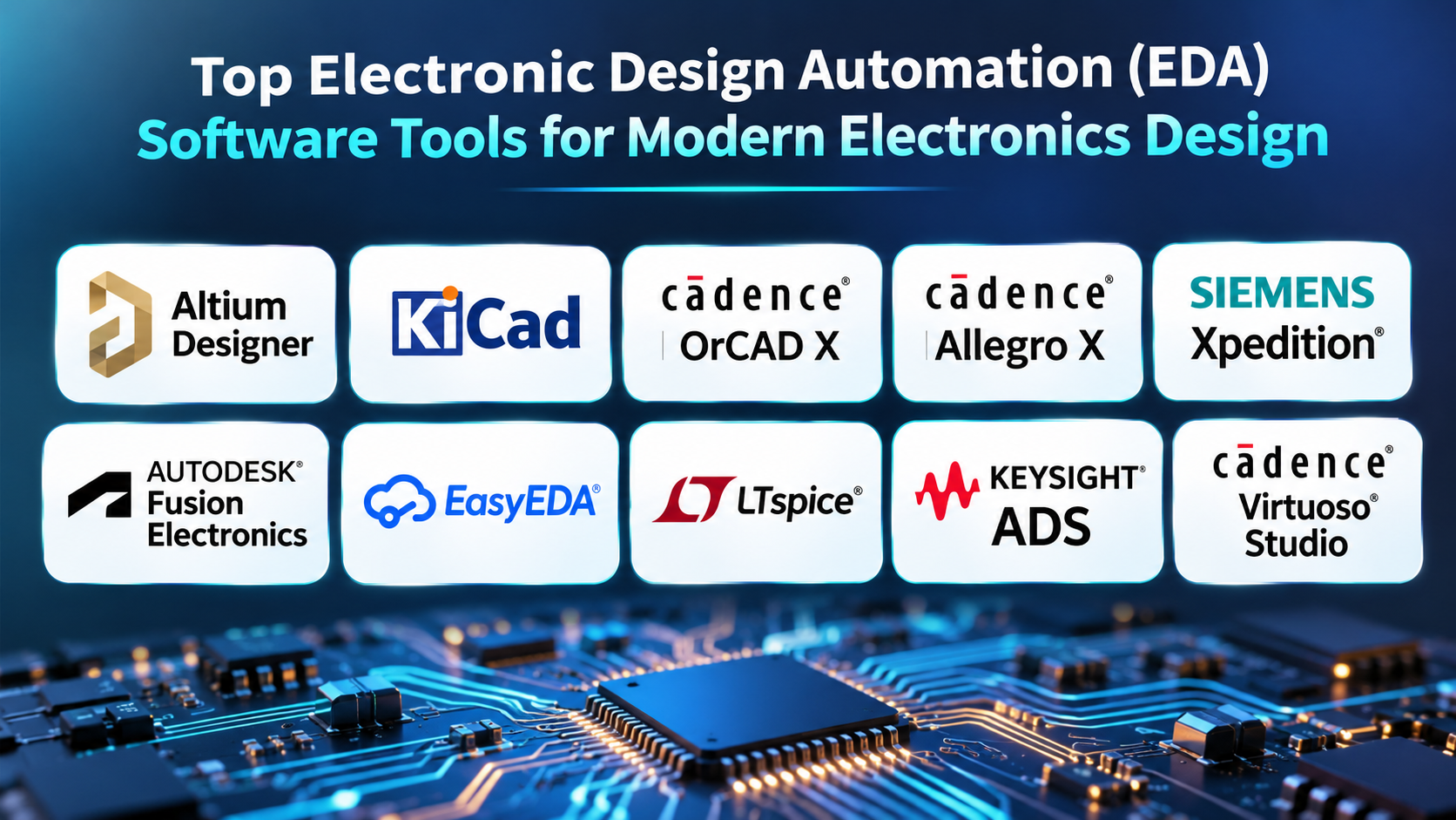
This guide explains 10 important EDA tools in detail. It covers their main features, common uses, strengths, and limits. It also compares them to help you find the right fit.
Understanding Electronic Design Automation Software
EDA stands for Electronic Design Automation. It refers to software that helps engineers design and check electronic systems.
A typical electronic product may need several design steps:
- Schematic capture: Engineers draw the circuit and show how components connect.
- Circuit simulation: They test circuit behavior before building a physical model.
- PCB layout: They place components and create copper paths between them.
- Design verification: They check the design for electrical and manufacturing errors.
- Manufacturing preparation: They create files and documents for board production.
Chip design follows a different path. Engineers create and check circuit layouts inside an integrated circuit. RF design also needs special tools to study high-frequency signals.
One EDA package may cover several steps. Another may focus on just one. So, the tools below are not all direct competitors.
1. Altium Designer
Best for: Professional PCB design
Altium Designer is a professional electronic design platform. It helps engineers turn circuit ideas into complete PCB designs.
The software connects schematic design, PCB layout, routing, and manufacturing preparation. This means engineers can manage many design steps in one place.
How Altium Designer Works
Engineers usually begin with a schematic. They add electronic parts, such as resistors, capacitors, chips, and connectors. Then they draw the connections between those parts.
Next, they move the design into the PCB editor. The editor helps them arrange components on the board. Engineers then create copper tracks that connect the parts.
Altium Designer keeps the schematic and PCB layout linked. So, when engineers change a connection, they can review that change in the board design.
The software also offers interactive routing. This helps engineers guide copper tracks around components and other tracks. Design rules help check spacing, track width, and other layout limits.
Its 3D view lets engineers inspect the board from different angles. They can also review component placement and board shape before production.
Main Features
- Schematic capture for circuit diagrams.
- PCB layout and interactive routing.
- Design rule checking.
- 3D PCB viewing.
- Rigid-flex PCB design support.
- Component and parts information.
- Manufacturing file generation.
- Design review and collaboration tools.
Where It Is Useful
Altium Designer works well for consumer electronics, industrial devices, control systems, and connected products.
It can help teams that build multi-layer boards. It also suits projects that need clear design records and repeatable manufacturing files.
Pros
- Combines schematic and PCB design.
- Offers advanced routing tools.
- Supports complex board layouts.
- Provides 3D board inspection.
- Helps prepare manufacturing files.
- Supports design reviews and team workflows.
Cons
- Commercial licensing can cost a lot.
- Beginners need time to learn the interface.
- Advanced projects need careful library management.
- Small projects may not need all its features.
Our View: Altium Designer is a strong option for professional PCB development. It makes sense when a team needs a connected design process. Smaller projects may get enough value from a free or simpler tool.
2. KiCad
Best for: Free and open-source PCB design
KiCad is a free, open-source EDA software suite. It helps users create circuit diagrams and printed circuit boards.
The software includes separate tools for schematic design and PCB layout. These tools work together to keep circuit connections and board design aligned.
KiCad is popular with students, hobbyists, engineers, and small product teams. It offers a useful set of design tools without requiring a paid commercial license.
How KiCad Works
A project often starts in the schematic editor. Users select parts from libraries and place them on a drawing sheet. They then connect the parts to show how the circuit should work.
After completing the schematic, users move to the PCB editor. KiCad transfers the circuit connections into the board design. Users can then arrange component footprints and route copper tracks.
A footprint shows the physical connection pattern for a component. It tells the PCB layout where to place pads, holes, and other connection points.
KiCad also includes a 3D viewer. This lets users inspect the board with component models. It can help reveal placement or clearance problems before manufacturing.
The suite includes useful extra tools. These include a Gerber viewer, a PCB calculator, and SPICE simulation support. The tools help users review board files and study circuit behavior.
Main Features
- Schematic capture.
- PCB layout and routing.
- Electrical rule checking.
- 3D board viewing.
- Symbol and footprint libraries.
- Gerber file viewing.
- PCB design calculations.
- SPICE circuit simulation support.
- Manufacturing file export.
Where It Is Useful
KiCad suits educational projects, prototypes, open-source hardware, and small commercial products.
It can also support more complex boards. However, teams should test their own workflows and design needs before adopting it for large projects.
Pros
- Free and open-source.
- Runs on Windows, Linux, and macOS.
- Supports schematic and PCB workflows.
- Includes a 3D board viewer.
- Offers useful design libraries.
- Has a large user community.
- Gives users control over project files.
Cons
- Beginners may need time to learn it.
- Some library work needs manual care.
- Team workflows may need extra tools.
- Users must check footprints before production.
- Advanced commercial workflows may need other systems.
Our View: KiCad is one of the strongest options for users who want capable PCB design software without license fees. It is a good starting point for learning EDA. It can also support serious design work when teams manage libraries and manufacturing checks carefully.
3. Cadence OrCAD X
Best for: Professional circuit and PCB workflows
Cadence OrCAD X is a PCB design platform for engineers and electronics teams. It brings circuit capture, PCB layout, simulation options, and manufacturing preparation into a connected workflow.
The platform helps engineers move from a circuit idea to a board design. It also supports design checks and component information during development.
OrCAD X is useful for teams that need more control over their PCB projects. It can support both smaller product teams and demanding electronic designs.
How OrCAD X Works
Engineers begin by creating a schematic. They place components and define the electrical connections between them.
The schematic then connects to the PCB layout. Engineers arrange the parts and route tracks based on the board’s design rules.
OrCAD X supports constraint management. Constraints are rules that control how a board must be designed. For example, they can set track widths, spacing, and signal requirements.
The platform also offers design checks during the layout process. These checks help engineers find problems before they send a board for production.
OrCAD X includes connections to simulation and analysis tools. Its wider Cadence environment can support mixed-signal simulation and signal integrity work. The exact tools available depend on the product setup and license.
Main Features
- Schematic capture.
- PCB layout and routing.
- Electrical rule checking.
- Constraint management.
- Mixed-signal simulation options.
- Component and supply information.
- Manufacturing documentation.
- Collaboration and design review.
Where It Is Useful
OrCAD X suits product development teams that design control boards, embedded systems, industrial electronics, and consumer devices.
It can help teams that need a clear link between schematics and PCB layout. It is also useful when engineers want to connect PCB design with other Cadence tools.
Pros
- Connects schematic and PCB design.
- Supports design rule and constraint checks.
- Offers links to simulation tools.
- Helps manage component information.
- Supports manufacturing preparation.
- Provides collaboration options.
Cons
- Commercial licensing can be expensive.
- The platform takes time to learn.
- Some advanced tasks need additional tools.
- Teams may need training before full use.
Our View: OrCAD X is worth considering for professional PCB development. It offers a connected workflow without requiring every team to use the same advanced enterprise setup. Buyers should confirm which analysis and collaboration features their selected package includes.
4. Cadence Allegro X Design Platform
Best for: Complex and high-speed PCB systems
Cadence Allegro X is designed for demanding PCB and electronic system projects. It helps engineers manage complex boards, detailed routing rules, and advanced electrical needs.
High-speed boards need careful signal control. Signals can lose quality when tracks run too close together or follow poor paths. Engineers must consider timing, impedance, and signal interaction.
Allegro X provides tools to help manage these issues. It supports design checks, routing, analysis, and team workflows.
How Allegro X Works
Engineers create or import the circuit design. They then define board layers, component positions, and routing rules.
The PCB editor helps them place components and connect the required signals. Its routing tools support detailed control over copper tracks.
The platform also supports advanced interfaces. Engineers can work with timing and phase tuning features for designs that need careful signal matching.
Allegro X connects with analysis tools in the Cadence environment. These can help engineers study signal integrity and power delivery. The wider platform also supports electrical, mechanical, and thermal design work.
Its collaboration tools can help teams work on shared designs. This matters when several engineers handle schematic capture, placement, routing, and review.
Main Features
- Advanced PCB layout and routing.
- Constraint-based design.
- Electrical rule checking.
- Signal and power integrity analysis options.
- High-speed interface tuning.
- Multi-board and system-level design workflows.
- Team collaboration.
- Manufacturing checks and documentation.
Where It Is Useful
Allegro X suits high-speed computing boards, networking hardware, automotive electronics, and complex industrial systems.
It is useful when the board has many layers, dense components, or strict signal requirements.
Pros
- Supports complex PCB layouts.
- Offers advanced routing controls.
- Helps manage high-speed design rules.
- Connects with analysis tools.
- Supports team-based design.
- Provides manufacturing checks.
Cons
- Requires strong PCB design knowledge.
- Licensing and setup can be costly.
- Training may take significant time.
- Small boards may not need its advanced features.
Our View: Allegro X is a specialist choice for complex PCB work. It makes sense when signal quality, routing control, and design complexity matter. A smaller product team may find a simpler PCB tool easier to manage.
5. Siemens Xpedition
Best for: Enterprise PCB design
Siemens Xpedition is a scalable electronic systems design platform. It supports PCB design for independent engineers, growing teams, and large companies.
The platform connects schematic capture and PCB layout. Its wider product family also supports design automation, analysis, manufacturing checks, and collaboration.
One important part of Xpedition is its ability to support different team sizes. A smaller team may use a simpler product package. A large company may need broader design and analysis features.
How Xpedition Works
Engineers create circuit schematics and connect the parts. They then move the design into the PCB layout environment.
The PCB tools help them place components and route electrical connections. Design rules help keep the board within electrical and manufacturing limits.
Xpedition also supports library and design data management. This helps teams reuse approved parts and keep project information organized.
Large companies may use several design teams. Xpedition supports workflows that help these teams share information and manage changes.
Siemens also provides migration tools for teams moving from other PCB platforms. These tools can help transfer existing designs and libraries. Teams should still check migrated files before using them in production.
Main Features
- Schematic capture.
- PCB layout and routing.
- Design automation.
- Design rule checking.
- Manufacturing checks.
- Component and library management.
- Design analysis options.
- Team collaboration.
- Migration support.
Where It Is Useful
Xpedition suits automotive electronics, industrial equipment, communication systems, and large electronic product programs.
It can help companies that need to manage many projects and design teams. It also suits teams that want to connect PCB design with wider product engineering processes.
Pros
- Scales across different team sizes.
- Supports complex PCB design.
- Offers design and library management.
- Provides migration support.
- Connects design and manufacturing tasks.
- Offers options for analysis and collaboration.
Cons
- Advanced workflows need training.
- Licensing depends on the selected package.
- Setup can take time.
- Smaller teams may not need enterprise features.
Our View: Siemens Xpedition is a strong option for teams with complex design needs. Its product range gives companies room to expand their workflows. Buyers should compare the exact packages and add-ons before making a decision.
6. Autodesk Fusion Electronics
Best for: Combined electronic and mechanical design
Autodesk Fusion Electronics brings electronic design into the wider Autodesk Fusion environment. It helps engineers create circuit diagrams and PCB layouts while working with mechanical product models.
This connection is useful because a circuit board must fit inside a physical product. Engineers need to consider the enclosure, connector positions, mounting holes, and available space.
Fusion helps teams review these details during product design. This can reduce problems that appear when electronic and mechanical designs come together late.
How Autodesk Fusion Electronics Works
The design process starts with a schematic. Engineers add components and connect them to describe the circuit.
They then move to the PCB layout. They define the board shape, place components, and route copper tracks.
The software keeps the schematic, 2D PCB, and 3D PCB documents connected. This helps users move between electrical and physical design views.
Engineers can check the PCB in the context of the mechanical enclosure. They can review connector positions and clearances before production.
Fusion also supports design rule checks and manufacturing output. It can generate files such as Gerber data, drill files, and assembly information.
Main Features
- Schematic capture.
- PCB layout and routing.
- 2D and 3D PCB design.
- ECAD-MCAD integration.
- Design rule checking.
- Component libraries.
- SPICE simulation support.
- Manufacturing file export.
- Thermal analysis options.
Where It Is Useful
Autodesk Fusion Electronics suits startups, product designers, and engineering teams that build physical products with electronic parts.
It can be useful for smart devices, connected equipment, robotics, and compact consumer products.
Pros
- Connects electronic and mechanical design.
- Helps check PCB fit inside an enclosure.
- Links schematics with board layouts.
- Supports 3D board inspection.
- Offers manufacturing file export.
- Includes component library tools.
Cons
- Specialist PCB teams may need more advanced tools.
- Users must learn the wider Fusion workflow.
- Feature access can depend on the plan.
- Complex projects need careful performance testing.
Our View: Fusion Electronics is useful when the PCB is only one part of a larger product. Its ECAD-MCAD link can help teams catch physical fit problems early. Teams focused only on advanced PCB routing should also compare specialist PCB platforms.
7. EasyEDA
Best for: Browser-based PCB design
EasyEDA is an online electronic design tool. It helps users create schematics and PCB layouts through a web-based environment.
The software aims to make PCB design easier to access. Users can work with component libraries and share projects online.
EasyEDA also connects with electronics parts and PCB manufacturing services. This can help users move from design to production without building every part of the process themselves.
How EasyEDA Works
Users begin by creating a schematic. They choose components from the available libraries and connect them.
After checking the circuit, they can convert the schematic into a PCB layout. The software transfers the component connections into the board design.
Users then define the board outline and arrange the components. They route copper tracks and check the design against layout rules.
EasyEDA also supports custom footprints. A footprint describes the physical pads and connection points for a component. Users can edit an existing footprint or create one when needed.
The platform supports online sharing and team cooperation. It also offers ways to import designs from other EDA tools. Users should check format compatibility before moving important projects.
Main Features
- Browser-based schematic capture.
- PCB layout and routing.
- Component libraries.
- Custom footprint creation.
- Design rule checking.
- Online project sharing.
- Team collaboration.
- Manufacturing file export.
- Links to component and PCB services.
Where It Is Useful
EasyEDA suits students, hobbyists, makers, and small product teams.
It can help users create simple boards and early prototypes. It is also useful for people who want to access their projects through a browser.
Pros
- Offers a browser-based workflow.
- Provides a free entry option.
- Includes component libraries.
- Supports schematic-to-PCB conversion.
- Allows online sharing.
- Connects with manufacturing services.
Cons
- Some workflows depend on online services.
- Advanced users may need more specialist features.
- Cloud storage may not suit every company.
- Users should check library and footprint quality.
- Project migration needs careful testing.
Our View: EasyEDA is a practical starting point for learning PCB design. It can also help makers and small teams create prototypes. Companies with strict data rules should review its cloud and project-sharing policies first.
8. LTspice
Best for: Analog circuit simulation
LTspice is a circuit simulation tool from Analog Devices. It helps engineers test how analog circuits may behave before they build them.
Unlike a full PCB design platform, LTspice focuses on simulation. It helps users study voltage, current, timing, and other electrical results.
This makes it useful during the early design stage. Engineers can test circuit ideas and adjust component values before building a physical prototype.
How LTspice Works
Users draw a circuit using the schematic editor. They add components and connect them with wires.
Next, they set the values and models for the parts. They choose the type of simulation they want to run.
LTspice calculates how the circuit behaves under the selected conditions. Its waveform viewer displays the results as graphs.
For example, an engineer can study how a power supply responds to changes in load. They can also test filters, amplifiers, and switching circuits.
Simulation results depend on the models and assumptions used. Engineers should compare important results with real measurements before approving a final design.
Main Features
- SPICE circuit simulation.
- Schematic capture.
- Waveform viewer.
- Analog circuit analysis.
- Component models.
- Example circuits.
- Support for Windows and macOS.
Where It Is Useful
LTspice suits analog engineers, students, power electronics designers, and circuit developers.
It can help with power supplies, filters, amplifiers, and other analog circuits. It is also useful for learning how component values affect circuit behavior.
Pros
- Free to use.
- Designed for analog simulation.
- Includes a schematic editor.
- Offers a built-in waveform viewer.
- Provides example circuits and models.
- Helps test ideas before prototyping.
Cons
- Does not replace a full PCB layout tool.
- Beginners need to learn simulation settings.
- Results depend on model quality.
- Some component models need extra setup.
- Simulation does not replace physical testing.
Our View: LTspice is a valuable tool for circuit analysis. It works especially well when engineers need to test analog behavior. Pair it with a PCB design tool when you need to create a physical board.
9. Keysight Advanced Design System (ADS)
Best for: RF and high-speed electronic design
Keysight Advanced Design System, known as ADS, is a specialist EDA platform. It focuses on radio-frequency, microwave, and high-speed electronic systems.
These systems need careful signal analysis. At high frequencies, circuit behavior can change because of electromagnetic effects, signal loss, and unwanted coupling.
ADS helps engineers study these effects before building hardware. It combines circuit simulation with electromagnetic and electro-thermal analysis.
How ADS Works
Engineers create a circuit or system model. They add components and define the connections between them.
They can then run simulations to study electrical behavior. For RF projects, they may examine signal gain, frequency response, and other important results.
ADS also supports electromagnetic simulation. This helps engineers study how physical structures affect signals.
The platform can analyze circuits, boards, packages, and interconnects. This is useful when a design includes several connected technologies.
ADS also supports Python automation. Engineers can use scripts to automate parts of their design and simulation work.
Main Features
- RF and microwave circuit design.
- High-speed digital analysis.
- Electromagnetic simulation.
- Circuit and EM co-simulation.
- Electro-thermal analysis.
- Signal and power integrity tools.
- Advanced packaging workflows.
- Python automation.
- Design optimization.
Where It Is Useful
ADS suits wireless communication, RF modules, microwave systems, high-speed digital boards, and advanced electronic packaging.
It can help engineers working on antennas, amplifiers, transceivers, and high-frequency circuits.
Pros
- Offers specialist RF design tools.
- Combines circuit and electromagnetic simulation.
- Supports high-speed digital analysis.
- Helps study complex signal behavior.
- Supports automation through Python.
- Covers several advanced design areas.
Cons
- Has a steep learning curve.
- Commercial licensing can be costly.
- Requires specialist engineering knowledge.
- May be excessive for basic PCB projects.
- Complex simulations need careful setup.
Our View: Keysight ADS is a specialist platform for demanding electronic systems. It is a strong option when RF, microwave, or high-speed signal behavior matters. It is not the first choice for simple circuit board projects.
10. Cadence Virtuoso Studio
Best for: Custom integrated circuit design
Cadence Virtuoso Studio is a specialist platform for custom integrated circuit design. Engineers use it to develop analog, RF, and mixed-signal chips.
An integrated circuit contains many electronic components inside a small semiconductor structure. Designing one requires tools that work at a much smaller scale than ordinary PCB design.
Virtuoso Studio helps engineers create circuit schematics and physical chip layouts. It also supports analysis and verification during development.
How Virtuoso Studio Works
The process often begins with a circuit schematic. Engineers define the electronic components and how they connect.
They then create a physical layout. This step places circuit elements and connects them using the layers available in the chip manufacturing process.
The platform helps maintain the link between the schematic and layout. This matters because a physical layout must match the intended circuit.
Engineers can also study circuit behavior before and after layout. This helps them understand how physical effects may change performance.
Virtuoso Studio supports custom IC, RF, mixed-signal, photonics, and advanced heterogeneous design workflows. Some advanced tasks connect with other Cadence products and technologies.
Main Features
- Custom IC schematic design.
- Analog and mixed-signal design.
- Physical chip layout.
- RF design support.
- Circuit analysis and verification.
- Layout verification workflows.
- Advanced-node design support.
- Heterogeneous integration options.
- Photonics design support.
Where It Is Useful
Virtuoso Studio suits semiconductor companies, chip design teams, and research groups.
It is useful for custom analog chips, RF integrated circuits, mixed-signal systems, and advanced semiconductor products.
Pros
- Built for custom integrated circuit design.
- Supports analog and mixed-signal workflows.
- Connects schematic and layout tasks.
- Offers analysis and verification tools.
- Supports RF and photonics workflows.
- Works with broader Cadence design systems.
Cons
- Requires specialist chip design knowledge.
- Commercial licensing can be expensive.
- Setup and process design data can be complex.
- Not intended for ordinary PCB design.
- Advanced workflows may require other Cadence tools.
Our View: Virtuoso Studio is a specialist choice for custom semiconductor design. It is not a general PCB tool. Teams should consider it when they need detailed control over analog, RF, or mixed-signal chip development.
Comparison Table: Top 10 Electronic Design Automation Software Tools
| Software | Main Purpose | Best For | Main Strength |
|---|---|---|---|
| Altium Designer | PCB design | Professional PCB teams | Connected schematic and PCB workflow |
| KiCad | PCB design | Students, makers, and engineers | Free and open-source tools |
| Cadence OrCAD X | Circuit and PCB design | Professional electronics teams | Connected design and analysis |
| Cadence Allegro X | Advanced PCB design | High-speed and complex boards | Advanced routing and design checks |
| Siemens Xpedition | Enterprise PCB design | Large engineering teams | Scalable design workflows |
| Autodesk Fusion Electronics | PCB and mechanical design | Physical product development | ECAD-MCAD integration |
| EasyEDA | Online PCB design | Beginners and small teams | Browser-based design |
| LTspice | Circuit simulation | Analog circuit engineers | SPICE simulation and waveforms |
| Keysight ADS | RF and high-speed simulation | RF and microwave engineers | Circuit and electromagnetic analysis |
| Cadence Virtuoso Studio | Custom IC design | Semiconductor teams | Custom chip design and verification |
How to Choose the Right EDA Software
The right tool depends on what you want to design. Start with your project needs instead of choosing the most popular name.
1. Choose by Design Type
Different projects need different tools.
- PCB design: Consider Altium Designer, KiCad, OrCAD X, Allegro X, Xpedition, or EasyEDA.
- Electronic and mechanical product design: Consider Autodesk Fusion Electronics.
- Analog circuit simulation: Consider LTspice.
- RF and microwave design: Consider Keysight ADS.
- Custom chip design: Consider Cadence Virtuoso Studio.
2. Check Your Team’s Experience
Some tools suit beginners and small teams. Others need specialist knowledge.
KiCad and EasyEDA can help new users learn PCB design. Advanced platforms may need trained engineers and structured workflows.
3. Review the Full Cost
A software license is only one part of the cost. You should also consider training, support, hardware, and extra modules.
Free tools can still need time for setup and maintenance. Paid tools may offer features that help large teams manage complex projects.
4. Check File Formats and Compatibility
Your software must work with your design team and manufacturer.
Check support for common PCB outputs, such as Gerber files and drill data. Also review BOM, pick-and-place, and 3D exchange needs.
If you plan to move from another EDA tool, test file import and export first. Some design details may need manual review.
5. Test the Tool with a Real Project
A product demo may not show every issue. Try a small project that matches your real work.
Create a schematic, run checks, build a board, and export manufacturing files. Ask your team to review the process.
This helps you judge the software before making a long-term choice.
Common Mistakes to Avoid When Choosing EDA Software
- Choosing by popularity alone: A popular tool may not fit your design type.
- Ignoring simulation needs: Some projects need deeper circuit or signal analysis.
- Overlooking library quality: Incorrect footprints can cause board problems.
- Skipping manufacturing checks: A design must meet factory rules.
- Ignoring file compatibility: Old projects may not transfer perfectly.
- Buying more features than needed: Extra tools can raise costs and training time.
- Forgetting data security: Review cloud storage and access rules before sharing designs.
Frequently Asked Questions
1. What is Electronic Design Automation software?
EDA software helps engineers design and test electronic circuits, PCBs, and integrated circuits. It can also prepare files for manufacturing.
2. Which EDA software is free?
KiCad and LTspice are free tools. EasyEDA also offers a free option. Check each product’s current terms and feature limits.
3. Which EDA software is best for PCB design?
The right choice depends on the board and the team’s needs. KiCad offers a free option. Altium Designer, OrCAD X, Allegro X, and Xpedition serve professional workflows.
4. Is EDA software used for chip design?
Yes. EDA includes tools for integrated circuit design. Cadence Virtuoso Studio supports custom analog, RF, and mixed-signal chip development.
5. What is the difference between EDA and PCB design software?
PCB design is one part of EDA. EDA also includes circuit simulation, chip design, and other electronic design tasks.
6. Can beginners learn EDA software?
Yes. Beginners can start with KiCad or EasyEDA. Learning basic circuit theory will make the process easier.
7. Why do engineers simulate circuits before building them?
Simulation helps engineers study circuit behavior before making a physical prototype. It can reveal problems early, but real hardware testing remains important.
8. Can one EDA tool handle every design task?
Some platforms cover several design steps. However, specialist work may need separate tools. Chip design and RF simulation often need dedicated software.
Final Thoughts
EDA software helps engineers turn electronic ideas into real products. It supports circuit design, PCB layout, simulation, and chip development.
But each tool serves a different need. KiCad and EasyEDA offer accessible PCB design. Altium Designer, OrCAD X, Allegro X, and Xpedition support professional board workflows. Autodesk Fusion Electronics connects electronic and mechanical design. LTspice focuses on circuit simulation. Keysight ADS serves RF and high-speed systems. Virtuoso Studio supports custom chip design.
Before choosing, define your project and your team’s skills. Check the design features, file formats, licensing, and support. Then test the software with a real project.
The best EDA tool is the one that fits your design work. It should help your team create accurate, reliable, and manufacturable electronics.
Clarify the ranking criteriaAdd a clearer tool selection matrix